As electronics continue to pervade every aspect of our lives, electromagnetic compatibility (EMC) has become an increasingly vital consideration for PCB layout. Poorly designed PCBs can generate electromagnetic interference (EMI) that can lead to malfunctions, data loss, or even damage to sensitive equipment. Not only that, but EMC is also a regulatory requirement in many industries. Therefore, it is essential for companies like Chengdu Mengsheng Electronics Co., Ltd. to provide solutions for EMC and supply high-quality EMI filter products to ensure proper PCB layout design.
Optimal EMI PCB Layout Guidelines
The following are some best practices that companies like Chengdu Mengsheng Electronics Co., Ltd. put in place for optimal EMI PCB layout:
1. Keep conductors short: One of the main culprits of EMI is the length of conductors on the PCB. Therefore, the shorter the conductors, the less EMI is generated. To achieve that, circuit designers should aim to place components as close together as possible and reduce the use of long traces.
2. Grounding: PCB grounding is one of the most important aspects of EMI PCB layout. A good grounding system can provide a low-impedance current return path, reducing EMI. The rules for grounding include avoiding ground loops, using a solid ground plane, and connecting all ground connections to a central point.
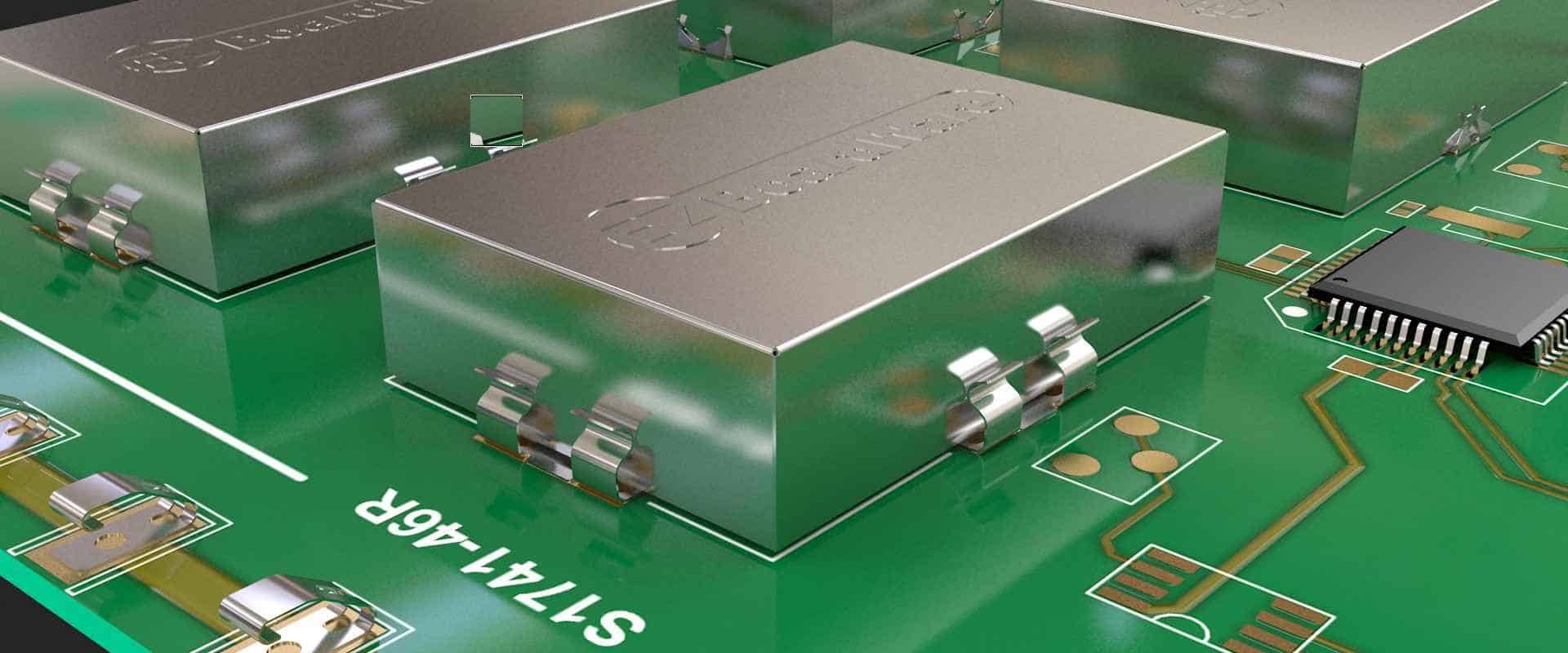
3. Shielding: Physical shielding can be used to block external EMI interference from entering the PCB, ensuring a clean signal. Shielding can be achieved by placing all sensitive components within a shielded enclosure or using conductive enclosures to surround the PCB.
4. Trace alignment: EMI is also affected by the alignment of the traces on the PCB. Traces that are routed side by side with opposing currents can generate EMI. Circuit designers should aim to keep high-frequency signals and power traces separated.
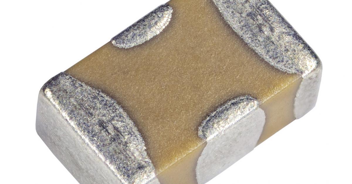
5. Properly placed capacitors and inductors: Capacitors and inductors can be used to filter out EMI. Placing these components correctly can reduce EMI and increase the PCB's reliability. Designers need to pay attention to the placement of these components and keep them as close to the relevant components as possible.
Benefits of Optimal EMI PCB Layout
Optimal EMI PCB layout provides several benefits for the designer, the manufacturer, and the end-user. These benefits include:
1. Better EMC compliance: Optimal PCB layout reduces the EMI generated by the PCB, ensuring that the final product meets EMC compliance regulations.
2. Reduced risk of malfunction: EMI can cause malfunctions in electronic devices. With optimal PCB layout, the risk of malfunction and data loss is reduced.
3. Enhanced product quality: Optimal PCB layout improves the product's quality, reducing the chances of a product recall, damage to sensitive equipment, and customer complaints.
4. Cost-saving: By ensuring a clean signal, optimal PCB layout reduces the likelihood of costly redesign and retesting, saving the manufacturer both time and money.
Conclusion
EMC is a necessary consideration in PCB layout design. Optimal EMI PCB layout guidelines help ensure that your PCB design meets requirements for electromagnetic compatibility and manufacturability. Chengdu Mengsheng Electronics Co., Ltd., with its vast experience in providing solutions for EMC, can assist in developing optimal PCB layout guidelines and supplying high-quality EMI filter products. By following the best practices outlined in this article, designers can improve the quality of their products, reduce malfunctions, and avoid costly redesigns. Contact Chengdu Mengsheng Electronics Co., Ltd. to get started on your optimal EMI PCB layout design today.